ORIGINALLY POSTED 15th October 2009
14,844 views on developerworks
This is a bit of an opus I’m afraid, but I’ve had my hands tied for so long in what I could / couldn’t say so think of this as a catch up for my last 6 months of sporadic posting! Please do try to make it to the end, I’m covering a lot here!
In my last post I covered whats coming with SVC 5.1 at a very high level. Over the next few posts I’ll be delving into the details. This post covers the new node engine hardware and the optional SSD features available. (This didn’t start as such an opus, but I’ve been biting my tongue for such a long time now about my experiences, thoughts and just what we’ve been up to with SVC)
CF8 Node Hardware
The CF8 node is the first to make use of Intels new Xeon 5500 (Nehelam) technology. Based on the same Nehelam core as Intels series of Core i5 and i7 desktop processors, CF8 comes with a single Quad core 2.4GHz CPU. Doesn’t sound much, but these beasts really are a huge leap forward over existing Xeons. The 2.4GHz is a middle to high end variant, using a embedded 1066MHz memory controller and running at 5.86GT (GigaTransations) on the new QPI (Quick Path Interface) that replaces the FSB (Front Side Bus). The change has been one for the better, no longer do memory requests and data have to flow over and flatten the FSB, likewise SMP traffic travels over another QPI. What we have found in general is that cache snooping traffic when running multiple dies (physical CPU packages) in a single box was always a bottleneck in older FSB technologies. Similarily, when benchmarking running say 2 cores on each of 2 dies, vs 4 cores on a single die (where the snooping is done on chip rather than over FSB/QPI) has a major benefit in throughput. SVC binds Fibre Channel ports to cores, and so each of the new 8 Gbit fibre ports in the current model is bound to its own core on the processor. There really is no need to have many tens of cores when you know how to squeeze every last MIP out of what you have. Similarily, we have been able to run FC ports at close to 100% utilisation for a long time. Many vendors only claim this should be avoided because of internal limitations… more in a min…
One of the things we are heading towards is more flexibility. Until now the SVC node hardware has been a fixed model, so an 8G4 was always an 8G4 and had the same internal hardware. With CF8, and beyond, we are moving away from this strategy, with various user feature upgrades becoming available over time. As I mentioned, we bind ports and cores and with the new QPI links to memory, like AMD CPUs , you now have memory that is “attached” or has affinity to a CPU. Thus, an obvious set of upgrades that we could make available in the future is to add a second Quad core, more memory and/or more ports. That said, the CF8 nodes we are shipping at GA are pretty much twice as powerful as the 2007 released 8G4 nodes which are being replaced. Hex and Oct cores aren’t that far off either…
Memory wise, we’ve moved to a 64bit kernel which allows us to address much larger virtual memory space, thus in the base CF8 node you will get 24GB per node – 192GB total cache in an 8 node cluster. We are only using 6 of the 16 DDR3 slots to get the 24GB, so upgrades in the future will likely allow 48GB and maybe even 96GB per node (when 8GB DDR3 is a sensible price!) One thing this does mean is that users with the original 2003 4F2 hardware cannot upgrade to 5.1 software as the Xeons in the 4F2 nodes are only 32-bit. We’ve always been proud that the software has always been backwards compatable with the hardware, but there comes a time when you have to move on. Users with 4F2 nodes that want to upgrade to get the 5.1 software enhancements should look to the Entry Edition 8A4 node we release last year. This is about double the performance of the 4F2 and as you already have the software license its simply a non-distruptive hardware upgrade… contact your account team or BP for more information.
On the buses, its all PCIe Gen2 – so double the internal bus bandwidth of the 8G4 nodes. Which nicely matches the doubled bandwidth we get from moving to 8Gbit Fibre ports. This gives a theoretical max throughput of a node pair of around 6.4GB/s – internal benchmarking has shown SVC 5 to deliver up to 6 GB/s – not far off the maximum when you consider the overhead of FC frames – and this was using my old 4Gbit AIX HBA ports, so added contention is going to detract from the maximums as well. The 8Gbit ports are on a single quad port card, based on PMC Sierra’s QE8 Tachyon. Internal to the box are two 16 lane PCIe risers, of which we are only using 8 lanes… at the moment…
In summary, yet again the original design decisions made back in 1999 to use commodity Intel based hardware has yet again proved to be the right decision. Another doubling in performance throughput per node, with little or no hardware development (from the SVC team) – even EMC have now seen the light and have switched to a commodity base for DMX-5 even if they are for now a generation behind on the CPU technology.
The two final changes for the basic hardware provide dual redundant power supplies (per node) and the move to a detachable display panel, using USB as its connection to the box (previous displays have simulated IDE and SATA as the interface) The display is detachable for a good reason…
Solid State Drive Upgrade Option

My regular readers will know that I’ve spent a lot of time over the last couple of years experimenting, benchmarking and generally thrashing various SSD products. I’ve learnt a lot about the raw technology as well as how different OEM suppliers have ‘solved’ some of the inherent inhibitors that had previously slowed the adoption of NAND flash as a real alternative to spinning rust. It became clear to us very early on that the two orders of magnitude improvement in IOPs throughput and order of magnitude better response time needed something a little special to enable a storage device to pass these improvements on to the applications using the storage. Yes, any decent storage system will be able to benefit from the improved response time, thats just a given. And while its great to improve response time for a couple of LUNs, if you can’t get every IOP from the SSD at the same time – hence achieve the more important $/iops, then the cost savings could be questioned. Now we (IBM) have put SSD devices into our existing storage systems – DS8000, DS5000 – where you can achieve much improved response times for those response time critical applications. You can even achieve much greater IOPs performance without needing to short stroke many HDD arrays, but its still not achieving maximal $/iops. EMC set the precedent for having that tick box in an enterprise array and we can do that too. However, SVC is setting the tick box for best $/iop, that is – we can drive SSD’s to their maximum potential – unlike any other high function storage system out there today. (I qualify this with high-function – so I don’t get bombarded by comments about TMS! – although their recent purchase of Incipient IP is an interesting move…)
This is a divergence for SVC, its the first time that the nodes themselves actually provide usable storage capacity. It may surprise a few people who have, quite sensibly, speculated that we’d be putting FusionIO based PCIe cards into the nodes as some kind of NetApp PAM style performance acceleration device. The truth is that to use SSD as a cache isn’t really what its all about.
Lets think about it for a minute. What is a cache. Its a mechanism by which storage systems have traditionally accelerated writes by, well caching them, and destaging later. Caches also accelerate sequential reads by prefetching them. But caches are really about making an HDD sequential seek arm look more like a true random access device (with constant latency – in this case rotational and seek time). However, ultimately a cache is all about bandwidth, bandwidth, bandwidth – and then of course we have to think about BANDWIDTH.
Todays SSD devices, even a PCIe based card has at least one order of magnitude (if not two) less bandwidth than RAM. So unless you have a very large amount of SSD (compared to RAM) and then a proportionally larger amount of HDD this doesn’t make sense. With RAM prices so cheap these days, a cache still makes sense to be RAM based. Thats why some form of automated fine-grained tiering, such as that provided by Compellent is a sensible way to think about bringing SSD devices to the market. These are after all still expensive, even though we’ve seen a pretty fast take down in price over the last year. All I can say regarding auto fine-grained tiering is that we have had ideas in this area for a long time. Until now, the difference in cost (when you weigh up all the costs associated with ‘housing’ an HDD) between FC and SATA has not meant such a function was really necessary.
On the subject, I do have to commend EMC marketing again – 18 months before you have a function, lets tell the market we have it, or at least it will be coming… mid-next year… FAST v1, isn’t as ground breaking as we are lead to believe. Its what SVC has had the ability (functionally) to do since initial release in 2003. Earlier this year, March, IBM Tivoli Storage Productivity Center (TSPC) released a new version which includes Intelligent Performance Optimizer (IPO). This produces a heat map of your enterprise and can therefore determine which LUNs are busiest, this ties in with knowledge of what response times should be, and can provide a set of recommendations as to what to move. It even produces a script of SVC migration commands that can be run to semi-auto migrate the data. In general we’ve found that end users don’t want the system to just move data without some kind of acknowledgment, or at least some kind of validation that the function does what it proclaims to. So IBM has been able to provide an equivalent to FAST v1 since March this year.
Anyway, we used the FusionIO cards last year with our project Quicksilver as it was a very simple development project to take the SVC code and turn it into a controller (we already use SVC to simulate storage in test) and access the ioDrives as a SCSI block device. For an integrated storage system however, this would mean taking a very large box, to enable lots of PCIe slots, and how would you non-disruptively replace one with ease.
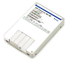
That, and the other reasons I outlined in my previous post, is why we’ve been working with STEC just as long as EMC have. Look back to my post in September 2007… SVC is the first SAN storage system to use their new SAS ZeusIOPs devices. We’ve also moved to the 2.5″ or SFF (Small Form Factor) drives. Now it becomes clear why we need a removable display panel. Hidden behind it are the SFF drive bays – integral to the 1U node hardware. We need our boot device and some retention brackets etc, so that leaves 4 drive bays for integrated SSDs. You can scale this from 1 through 4 per node – the only loose rule being that you should add SSDs in pairs – spread over the two nodes in an IO Group for redundancy purposes. This is a much cheaper entry point to use SSD storage than other RAID based solutions.
We all know SVC performs well and can produce some amazing IOPs numbers – just recently an ex-EMC salesman, now working with our XIV sales team sent me very nice email just after he’d seen SVC in action for the first time – something along the lines of “no wonder I didn’t have any luck trying to sell Invista…” We have the horsepower, but we needed a very fast SAS interface. I’d already discovered that nobody actually made one, because I’d been trying to benchmark various SAS and SATA STEC drives for some time, and constantly hit about 10K iops limits. Its the same problem as I described above. The storage industry has been driven to produce systems that hide the fact that we have spinning seek sensitive HDD devices backing everything. Until now, nobody has needed such high performance – except SVC – where we had to be able to process I/O for many many storage controllers virtualized under the appliance.
Our good working relationship with PMC Sierra meant it was quite simple to take their new SAS II (SPC) ASIC and build a “High performance SAS Adapter” as the feature is called. This is an 8lane PCIe Gen2 card capable of over 125K iops. More than enough to saturate a good number of STEC ZeusIOPs devices. So now we had the interfaces, the devices and of course we added Vdisk mirroring last year. We now can use this (and its read preference scheme) to sustain over 250K IOPs from a single node pair. At the same time we all know that writes and mixed workloads are a lot less per SSD, so we can comfortably saturate the SSDs with room for future expansion.
In a later post I will go on to explain more about the configuration options – for example we can mirror between SSD and HDD for acceleration of (the most common OLTP workload) read biased workloads, while getting every IOP from the SSD and doubling the available capacity (and double the effective $/iop).
In summary, this is different. It not just another storage system adding some SSD capacity, this is the highest end of the high end. You need up to 75K OLTP IOPs from one LUN, but at the same time don’t need huge capacity, why pay for huge numbers of HDD or SSD to get that, when 4 or 8, in the most highly efficent system will give you just that.
| Per SSD | Per IO Group (Mirrored SSDs) | Per Cluster (Mirrored SSDs) | |
|---|---|---|---|
| Raw Capacity | 146GB | 1168GB | 4672GB |
| Read 4KB IOPs | 35,000+ | 200,000+ | 800,000+ |
| Mixed 4KB IOPs (70/30) | 19,000 | 83,000 | 333,000 |
PS. Before those of you that know the “raw capability” of the ZeusIOPs SSD devices cry wolf and suggest that the base devices aren’t capable of what we are claiming here… think about what would happen if you could make a mixed workload not look like a mixed workload… wouldn’t that change what you could get from the device… oh yes… more later


Leave a comment